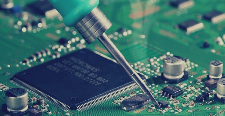
Regardless of whether you have been tasked to design and build a PCB or you just want to learn more about the process, there are some important things to know.
Controlled depth drilling
During PCB fabrication and design, there are several issues which need to be addressed. One of the most common is signal integrity. This can be achieved by using a technique known as back drilling. Using back drilling will improve the performance of a PCB. This technique works by removing unwanted stubs from vias.
The best part about this technique is that it doesn’t have a negative effect on the performance of a PCB. It can be applied to any type of PCB.
This process also reduces the number of bit mistakes per unit of time. This is important because the PCB board transmits signals through multiple layers. It can also reduce the total signal BER.
The most common PCB boards have through-holes that connect the layers of the PCB. These holes are drilled from top to bottom, allowing signals to flow between layers.
Laser direct imaging
LDI is a highly automated imaging process used for PCB design and fabrication. It uses a computer-controlled laser beam to produce a precise image. This image is matched to a pre-loaded CAD/CAM design file.
The laser beam is highly focused and able to image fine lines of less than two mils. This makes it ideal for handling small, fine trace widths. It is also a cheaper alternative to screen printing.
It is also easier to use than traditional imaging. The process eliminates the need for environmental chambers and phototools. It also eliminates light refraction. This allows the user to have more precise image positioning and image positioning accuracy.
The laser direct imaging process is a cost effective way to manufacture fine line PCBs. Because the process is automated, it is not affected by alignment issues associated with traditional photoplotter tooling methods.
Electroless nickel immersion gold
Among the many finishes that are available in the PCB industry, Electroless Nickel Immersion Gold (ENIG) is a common choice for PCB manufacturers. It features a two-layer metallic finish that provides a high-quality surface for soldering.
ENIG also provides a smooth, flat surface. This makes it easier for soldering components to bond. In addition, it provides exceptional electrical continuity and EMI shielding. It is also lead-free, which is ideal for lead-free soldering applications. It is also RoHS compliant.
Its thick and flat surface helps prevent oxidation. It also contributes to the excellent solderability of copper contacts. Consequently, it is ideal for a wide range of applications.
It is also ideal for IC package PCB substrates. It is immune to black nickel and can withstand multiple lead-free reflow soldering cycles.
Lamination
Printed circuit board (PCB) lamination is an essential step in PCB design and fabrication. It is also an important element in ensuring the reliability and durability of electronic circuits. PCBs must be laminated with the correct materials.
A laminated circuit board is a PCB that is laminated with multiple layers of prepreg or resin material. The prepreg serves as the glue for the laminate, which then serves as the foundation of the circuit board.
During lamination, the prepreg resin flows into the voids of the adjacent copper layers. This void area decreases adhesive shear strength and affects the thermal transfer between the PCB and the heat sink. It also decreases the bond strength.
Multilayer PCBs are commonly used to reduce product density. This is done by stacking multiple layers of prepreg or resin material together. They are then laminated together under extreme pressure and temperature. These laminates must be fabricated using materials with accurate thermal and mechanical properties. They also need to be fire-retardant, tough chemical resistance, and have good humidity resistance.

